Introduction
Etching is a subtractive method used for the production of etched circuit boards: acid is used to remove unwanted copper from a prefabricated laminate. This is done by applying a temporary mask that protects parts of the laminate from the acid and leaves the desired copper layer untouched.
Different machines and chemicals can be used for etching, which will affect the comfort, duration and quality of the result. Two Acid types that can be used for etching are ferric chloride and Sodium Per-sulphate. Although etching can also be done in simple plastic boxes, the quality of the results will improve when using a machine that controls temperature and constantly keeps the fluids in motion. There are small etching tanks with heating and air pump and there are small spray etching machines which can handle bigger PCBs and even the development and cleaning processes involved. The sprayer also decreases the etching time and the amount of acid needed.
Etching process
1. Designing the circuit board and producing a pdf of the design.
I design the circuit board shown below using KiCad. KiCad is a free software suite for electronic design automation (EDA). It facilitates the design of schematics for electronic circuits and their conversion to PCB designs. Check out these KiCad Tutorials. After designing the boards, I produced a pdf of the designs and printed the pieces on A4 papers with toner (photograph papers(mate)) so as to facilitate the next step in the process.
/oll7.png)
Circuit layers(Left: prototype 1 - layout, Right: prototype 2 - layout(includes footprints of some power analysis sensors)).
2. Transferring the design onto the PCB.
The circuit layout is printed with a laser printer on paper (with toner (photograph paper)), put face-down on the laminate, and the toner is transferred from the paper to the copper using an iron. The print must be of a very good quality, little mistakes we usually tend to ignore in printed text can result in unusable traces or even cause short circuits. The transfer of the toner is a bit tricky as well. If temperature is too high, the toner gets too liquid and the tracks will blur. If the temperature is too low, the toner won’t stick to the copper. After the ironing you can’t pull the paper away just like that, without destroying half of the mask. Instead you have to put the laminate with the paper in a water bath and wait a while until you can start to cautiously scrub away the paper.
/oll8.png)
Left: Circuit layout on the copper board/laminate after the transfer from the paper, Right: Etching with Aluminum III Chloride (AlCl3).
3. Etching.
CAUTION :Wear Protective Equipment when handling etching chemicals(Ferric Chloride and Sodium Per-sulphate) (eye protection and hand gloves)
- Put the board in the acid tank for about 20 minutes until the copper traces are completely etched. You can tell that it’s finished when the board turns from opaque pink to transparent yellow (depends on the type of board you are using).
- Move the board into the rinse tank for a few seconds. You can also use an Isopropanol spray.
- Dry the board with a cloth.
/oll10.png)
Etching (a little stiring is required).
/oll12.png)
Left : Final product, Right: after placing the components.
4. Drilling
Drilling of the desired drill holes is done carefully so as not to scratch the copper tracks using the drill bit.
/oll11.png)
Drilling.
Final product after drilling..
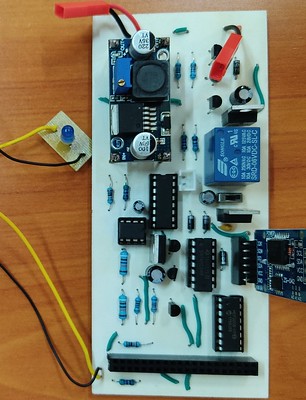
5. Project Ewaso prototypes (Prototype one and two)
After soldering / placing the components
/oll13.png)
Prototype 1 & 2.
Disadvatages of Etched Circuit Boards (Why etched boards are inferior to printed boards)
- The main disadvantage is, only the front and back copper layers can be etched the other important layers e.g.: the solder mask layer, the silk-screen layer,the paste layer etc. cannot be etched because they would appear as short circuits on the board.
- The other disadvantage is since the solder mask layer cannot be etched, it becomes difficult to use surface mount components (SMT, SMD). The solder mask layer is a very important layer because it is used to mount all surfaces mount components, the layer act as a link between the component leads and the copper footprint/track.
- Since drilling is done by hand in most etching cases the drilling precision is very poor. For printed circuit boards the drilling is done by a robot so the precision is very high.
- The other disadvantage is, double-sided board etching is quite hectic at the direct toner transfer stage. The transfer is done manually hence the etched product is prone to positioning errors between the front copper layer and the back copper layer.
- Since the etched copper tracks are exposed to stress and various damaging elements (corrosion) they do not last long as compared to the printed tracks.
- The etched copper tracks are not scratch resistance which is a problem when it comes to drilling and deployment of the final etched product.
- As the pitch decreases (distance from the centre of one pad to the centre of the adjacent pad) it becomes difficult to etch the foot print because the acid, in many cases do not get rid of the copper between the mounting pads. Such footprints can only be printed.
- High density circuit boards are difficult to etch because of reasons highlighted above.
- For a LOW PROFILE QUAD FLAT PACK (LPQF) microcontroller and microchip like the one shown below.
/oll14.png)
LOW PROFILE QUAD FLAT PACK (LPQF) microcontroller and microchip footprint.
Acknowledgement
- Mr. Johnathan Njiiru (PCB FABRICATION LAB - Dedan Kimathi University of Technology (DeKUT)).
- Centre for Data Science and Artificial Intelligence (DSAIL), Dedan Kimathi University of Technology